Home » Resources
Compass Technology Group Resources and Patents
The Compass Technology Group research and development team and engineers are continuously exploring new sensor technologies, cutting-edge radio frequency materials measurement equipment, and microwave non-destructive testing and evaluation systems to make equipment smaller, more powerful, and easier to use for industry. As we reimagine ways to test electromagnetic materials and components, we have filed for patents with the United States Patent and Trademark Office (USPTO). The team has also written multiple measurement standards, presented numerous papers on our work in innovative radio frequency (RF) materials measurement equipment, and have developed many videos showcasing our equipment.
Measurement Standards
The Free-Space Spot Probe Measurement Standard provides guidance for evaluating experimental or continuous production materials for electromagnetic applications. LEARN MORE
This test method evaluates reflection performance from experimental or continuous production materials in electromagnetic applications. LEARN MORE
This testing fixture measures the S-parameters of test specimens or witness coupons, along with appropriate calibration standards. LEARN MORE
The R-Coax Measurement Standard method evaluates the intrinsic properties of sheet materials, whether in small experimental batches or high-volume production, enabling non-destructive evaluation of materials in a manufacturing setting. LEARN MORE
The RF Capacitor Measurement Standard is a method for evaluating the intrinsic properties of bulk dielectrics (e.g. honeycomb or absorber foam) over a wide frequency range. LEARN MORE
This test method evaluates conductive materials used in electromagnetic shielding. LEARN MORE
Papers
This paper directly compares a laboratory focused beam system to an alternative measurement system based on recently developed RF spot probes. LEARN MORE
This paper compares a standard laboratory focused beam system to a measurement fixture based on AMMP spot probes that provides equivalent measurements with a more compact system. LEARN MORE
This paper introduces a fixture that simplifies the measurement of intrinsic properties for inhomogeneous and anisotropic dielectric materials at low frequencies. LEARN MORE
This paper describes an improved measurement method based on the parallel plate capacitor idea, which determines complex permittivity of dielectric sheets and films with thicknesses up to about 3.5 mm. LEARN MORE
This paper presents a reflectometer measurement method, along with example measurements of core slab materials, with two different inversion methods applied to these measured data. LEARN MORE
This paper describes a new correction method, which determines and corrects for phase and amplitude errors in transmission line cables. This technique does not require any specialized circuitry at the device under test (DUT). LEARN MORE
This article discusses the concept of a hand-held reflectometer system for the measurement of microwave relevant materials, integrating the microwave analyzer and sensor, thus eliminating the need for RF cables. LEARN MORE
This paper compares two different free-space extraction algorithms, developed for the simultaneous extraction of complex permittivity and permeability from metal-backed reflection. LEARN MORE
This paper describes the use of wide-band probes to interrogate a small area of a material or component and determine reflection or transmission properties in the 2 to 20+ GHz range. LEARN MORE
In this paper, the Compass Technology Group team presents an NDT method for detecting mechanical defects in radomes. LEARN MORE
This paper provides several new corrections that improve the loss tangent accuracy of free space methods over an order of magnitude. LEARN MORE
This paper presents a new flat lens antenna technology, which enables significant reductions in size and weight compared to conventional wide bandwidth horn antennas. LEARN MORE
In this paper, the Compass Technology Group team presents a new method for measuring thin polymer sheets using a slotted rectangular coaxial transmission line (R- Coax). LEARN MORE
This paper introduces a new, non-traditional, measurement method for obtaining complex dielectric properties at UHF and VHF frequencies. LEARN MORE
Videos
Test Methods
Focused Beam Fundamentals
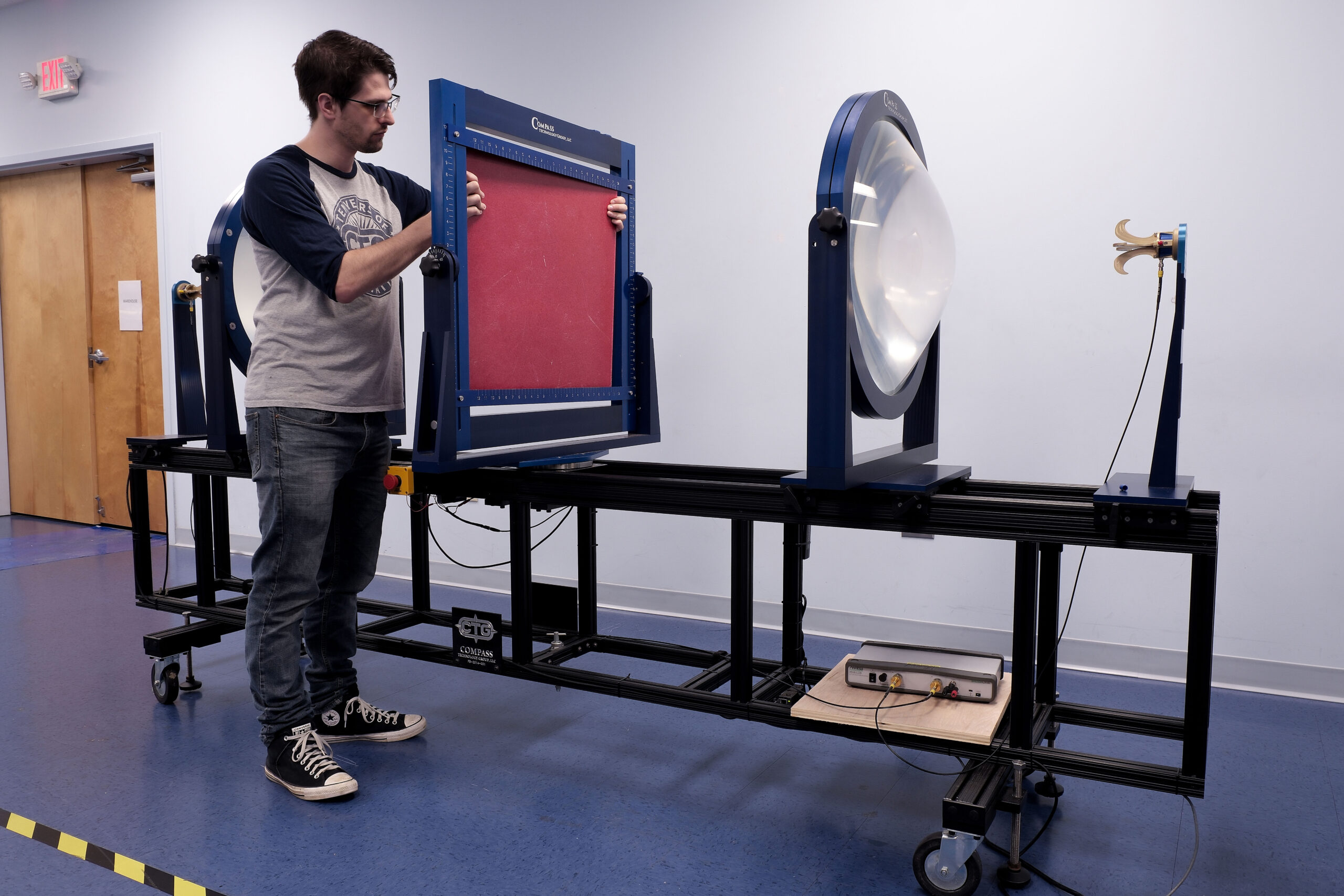
The focused beam technique uses lenses to focus free space energy onto a specimen. Measurement of transmission and reflection performance can then be used to invert intrinsic material properties. Watch this video to get an overview of the basic principles of microwave and millimeter wave focused beam measurements.
Focused Beam Shielding Effectiveness
The Compass Technology Group team has adapted the focused beam system to measure the shielding effectiveness of conductive materials. View this video to learn more about this method.
Copper Mountain Technologies Integration with Compass Technology Group’s Millimeter Wave Focused Beam System
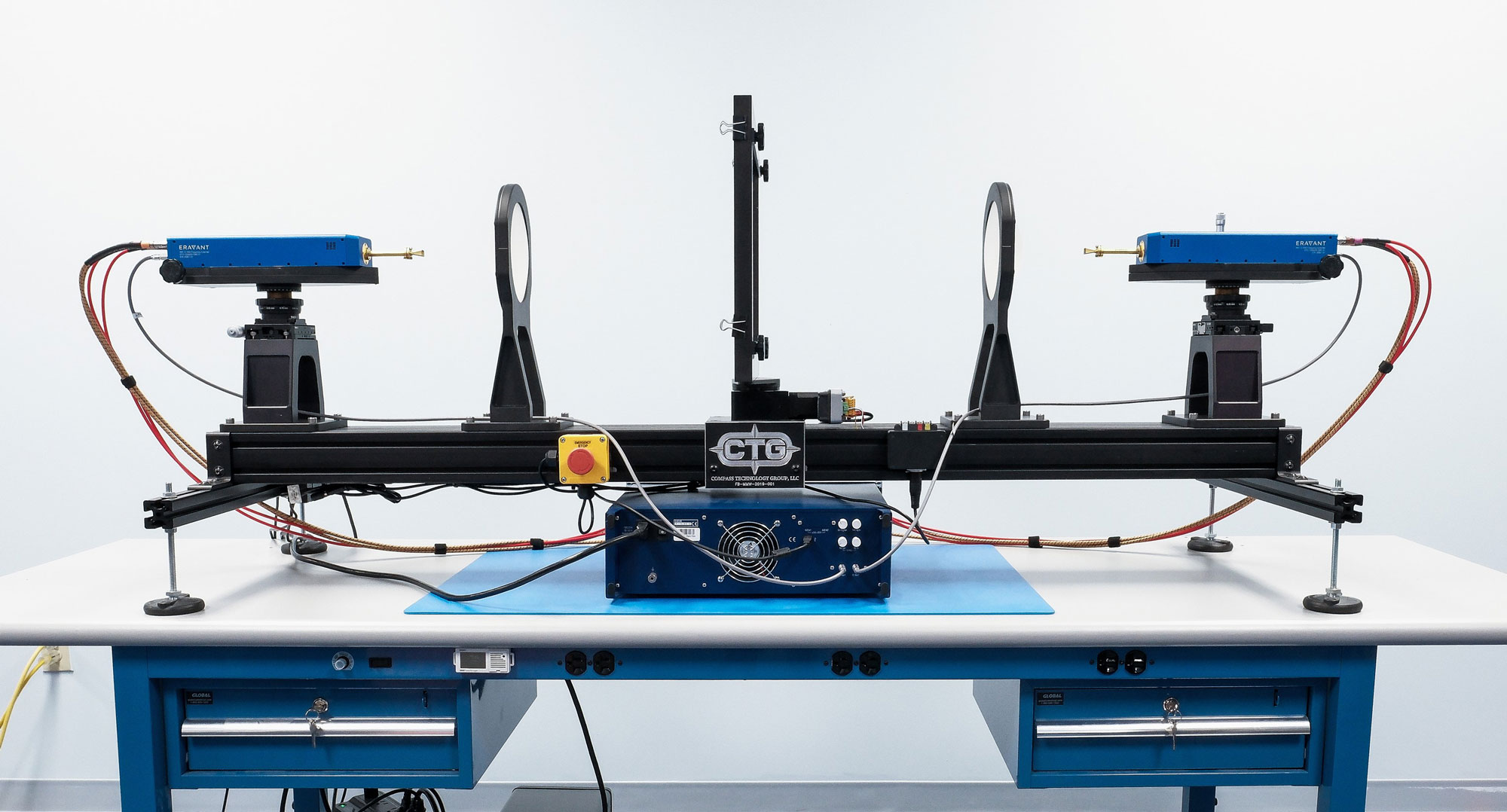
With the increasing use of millimeter wave frequencies for applications such as automotive radar and wireless communications, our team developed a focused beam lens system to conduct free space measurements at these frequencies. This video shows this system along with a Copper Mountain Technologies VNA and frequency extenders.
Anritsu Vector Star Integration with Compass Technology Group’s 2 GHz and Up Focused Beam
This video demonstrates how to measure a dielectric composite specimen using an Anritsu Vector Star VNA to drive a focused beam system.
Anritsu Shockline 1-Port Integration with a Cobot and the SP2040
In this demonstration video, the team pairs a 40 GHz 1-port VNA made by Anritsu with our 20 to 40 GHz spot probe. With a collaborative robot, we can automatically scan a radome and use the microwave map to identify defects.
Keysight PNA Integration with a Focused Beam Materials Measurement System
CTGcalc is Compass Technology Group’s software for collecting data, calibrating, and analyzing results. In this video, we use it to operate a four-port PNA from Keysight, which allows us to measure anisotropy in materials.
Patents
In this patent, various examples related to microwave dielectric analyzers and their use are provided. In one example, a microwave dielectric analyzer includes a measurement apparatus having a conductive electrode that can couple to a microwave analyzer and processing circuitry that can determine a dielectric characteristic of the dielectric specimen using a reflection coefficient measured by the microwave analyzer. The dielectric characteristic can be determined using a computational electromagnetic model of the measurement apparatus. The reflection coefficient can be measured by the microwave analyzer with the dielectric specimen in contact with the conductive electrode and/or sandwiched between conductive electrodes. The conductive electrodes can be axially aligned, and the second electrode may not be coupled to the microwave analyzer. Download the patent.
This patent contains various examples of methods and systems are disclosed for correction of phase and amplitude errors that occur in transmission lines connecting transmitter/receiver devices to measurement fixtures. In one example, a method is described that includes using time domain processing to determine a phase shift from the measurement fixture that can occur between calibration measurements and measurements of the specimen under test. In another example, a method is described that includes frequency-domain processing of the signals to obtain both phase and amplitude corrections. Including these phase and amplitude corrections in the calibration procedure can reduce or minimize the errors induced in the measurements when the transmission line(s) experience either temperature changes or physical deflections, among other things. Download the patent.
In this patent, examples are provided for fragmented aperture antennas. In one example, a fragmented aperture antenna includes a two-dimensional lattice of conducting elements, where positioning of the conducting elements in adjacent rows are offset based upon a fixed skew angle. In another example, a fragmented aperture antenna includes a two-dimensional lattice comprising a combination of first and second geometric conducting elements, where a second geometric conducting element provides a connection between adjacent sides of diagonally adjacent first geometric conducting elements. In another example, a fragmented aperture antenna includes a two-dimensional lattice of conducting elements having a single common non-rectangular shape, where the conducting elements interleave in a digitated fashion. Diagonally adjacent conducting elements overlap along a portion of adjacent edges of the diagonally adjacent conducting elements. Download the patent.
In this patent, you will see various examples of methods and systems are disclosed for non-contact determination of coating thickness. In one example, among others, a method includes illuminating a surface having a layer of a coating material with electromagnetic (EM) energy transmitted at two or more frequencies, obtaining measured reflection data from reflected EM energy, and matching the measured reflection data to modeled reflection data of a reflection model based upon minimization of an error between the measured reflection data and the modeled reflection data to determine a measured thickness of the layer. In another example, a system includes a probe configured to illuminate an area of the surface including a layer of a coating material with EM energy and receive reflected EM energy, and a processing device configured to determine a measured thickness of the layer based upon minimization of an error between measured reflection data and modeled reflection data. Download the patent.
An electromagnetic chamber absorber provided improved absorption across a wideband and both lower diffuse and specular scatter and a method for constructing the same. An exemplary device can compromise a periodic arrangement of disconnected electromagnetically lossy elements where the periodicity of the lattice is adjusted to suppress all or most grating lobe scattering. Because the electromagnetically lossy elements are disconnected, scalable manufacturing approaches are enabled. The lossy elements can be easily fabricated via shaping, which includes rolling, folding and cutting resistive and/or magnetic sheet materials. The lossy elements can be repeatably placed in a periodic lattice using low density scaffolding approaches and/or other alignment mechanisms. The absorption at the lower frequency part of the electromagnetic bands (below 1-2 GHz) can be improved via the addition of parallel lossy sheets into the low-density scaffolding. Download the patent.
Various examples of methods and systems are provided for traveling wave spot probes. In one embodiment, among others, a traveling wave spot probe includes one or more antennas positioned proximate to a coated surface. The one or more antennas can be configured to excite a surface traveling wave moving over an area under test by launching radio frequency (RF) energy at approximately a grazing angle to the coated surface under test. The one or more antennas can be positioned on a base placed proximate to the coated surface. The base can define the area of the coated surface under test. In another embodiment, a method for non-destructive testing of a coated surface includes positioning one or more antennas proximate to a coated surface and exciting a surface traveling wave over an area under test by transmitting RF energy via at least a portion of the one or more antennas. Download the patent.


